TROY TECHNICAL · BEGINNER’S GUIDE
READ THIS FIRSTSemiconductor assembly and packaging — An Introduction
Turn fabricated chips into products by connecting, protecting and cooling them.
Japanese version →Does fabricating a fast chip complete a computer? Signals still have to leave it, power must reach it, heat must escape and the assembly must survive use. Packaging is more than putting a chip in a box. It is part of designing a working system, especially when several chips must cooperate.
01Distinguish die, package and board
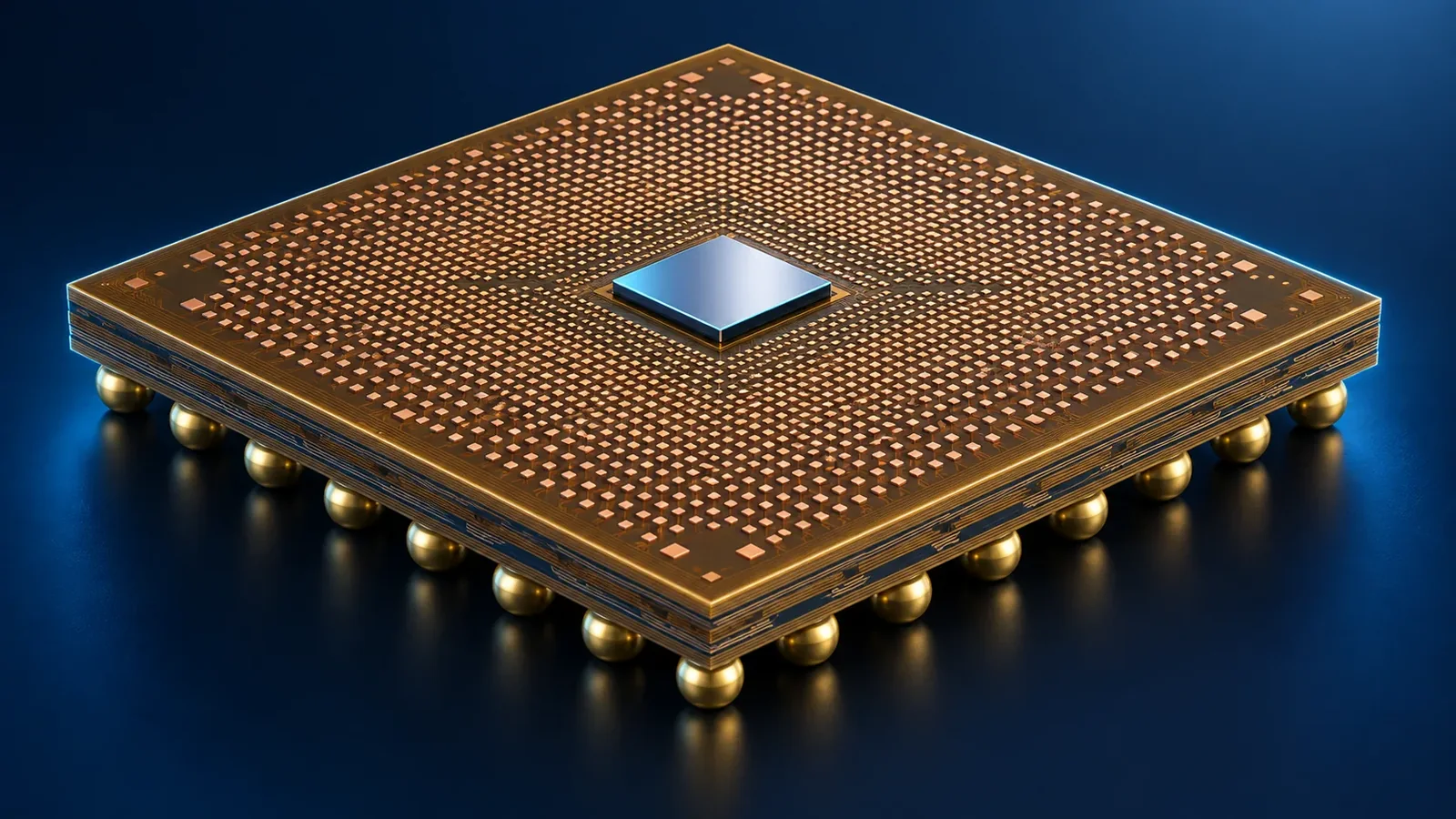
A die is a piece separated from a wafer carrying fabricated circuits. A package connects and protects one or more dies. That package is then attached to a printed circuit board. Keeping these levels separate prevents confusion over the word substrate.
A package substrate redistributes fine chip connections to a spacing usable by the outside assembly. Internal wiring and vias carry signals and power. An excellent die cannot overcome every bottleneck in these pathways.
Background: [1]
02Why not put everything on one enormous die?
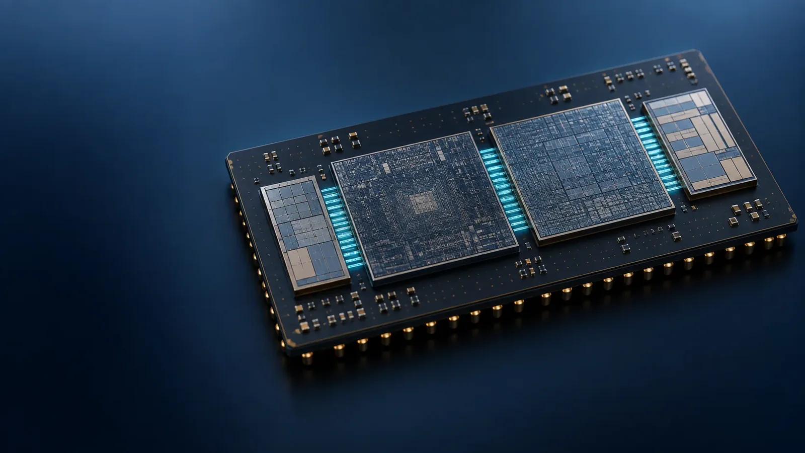
Compute, memory and input/output functions may favour different processes or materials. Chiplets split functions across smaller dies and connect them in one assembly. They fit within heterogeneous integration: combining separately manufactured components for a larger function.
This can enable reuse and more flexible process choices. It also introduces inter-die communication, assembly yield, testing and cooling challenges. Partitioning does not guarantee lower cost or higher speed; the complete design and test strategy decide the result.
Background: [2]
03Connect side by side, stack or bridge
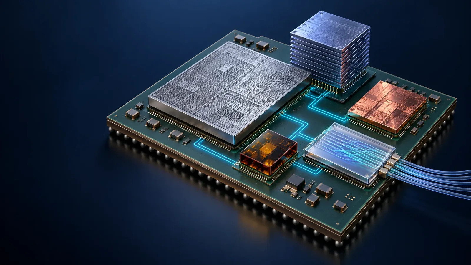
Chips can be connected side by side or stacked vertically. An interposer provides an intermediate routing layer; a bridge makes local connections; a through-silicon via, or TSV, provides a vertical path through silicon. These can coexist rather than being mutually exclusive choices.
Bumps are small connection structures. Hybrid bonding joins dielectric surfaces with metal interconnects. Increasing connection density or shortening wires brings requirements for alignment, surface quality, warpage control and testing.
Background: [1]
04Provide paths for heat and mechanical loads too
Powered chips generate heat. Short connections cannot help if heat trapped inside a stack limits operation. Thermal materials, lids and cooling systems belong in the design, as does stable power delivery.
Silicon, metals and polymers also expand differently with temperature. Concentrated mechanical loads can damage interconnects, so underfills and encapsulants support the assembly. These materials are not merely fillers for empty space.
Background: [1]
05Read the cross-section before comparing brand names
Names such as CoWoS, CoPoS and EMIB refer to vendor technologies or architectures. Comparing names alone can mix different levels: manufacturing formats, routing layers, bridges and stacks. Locate the dies and connection structures first, then consider bandwidth, power, area and reliability.
An advanced approach is not necessary for every product. A small sensor and a large AI system have different priorities. Follow structure first, then materials and manufacturing, before comparing named platforms.
Background: [3]
Connect the ideas in one situation
ILLUSTRATIVE SCENARIO — NOT A PERFORMANCE CLAIM
Suppose compute and memory need to be closer
More and shorter connections may help move data, but area, heat and power delivery still constrain the assembly. Stacking can shorten paths while making buried components harder to cool or test.
A defective component after assembly also raises a system-level question: what can be recovered? Considering performance, yield, test and repair together explains why several architectures coexist.
Return to the starting idea
Front-end fabrication makes devices and circuits; assembly and packaging connect chips into products. Signal, power, heat and mechanical loads must all have workable paths.
You do not need to memorize every technology name. Understanding the intended improvement, the mechanism being changed and the conditions needed to demonstrate it gives you a foundation for the detailed articles. Choose one route that matches your question.
Choose your next article
Read a route from top to bottom, or select just the question you need. You do not have to read everything.
Understand the assembly
Connections and assembly
Materials and platforms
Browse all technical articles in this field (31)
- What Co-Packaged Optics (CPO) Is
- What CoPoS Is
- What CoWoS Is
- EMIB and EMIB-T
- What High Bandwidth Memory Is
- What an OSAT Is
- What Panel Level Packaging (PLP) Is
- What an RDL Is
- What a System in Package Is
- What a Through-Silicon Via Is
- Underfill and Encapsulants
- What an Interconnect Is
- What an Interposer Is
- Wafer Thinning and Dicing
- What a Glass Substrate Is
- What Silicon Photonics Is
- What Die Stacking Is
- What a Chiplet Is
- What Semiconductor Test Is
- What Hybrid Bonding Is
- What a Bump Is
- What a Package Substrate Is
- What a Via Is
- What Buildup Film Is
- Fan-Out and WLP
- What Flip Chip Is
- Bridges and EMIB
- What Bonding Is
- Semiconductor Package Molding Why the “black resin” is a structural material (related-field guide)
- What the Coefficient of Thermal Expansion Is
- What Heterogeneous Integration Is
Sources and scope
This introductory synthesis connects the existing technical articles. Its grouping and design scenarios are explanatory, not standard classifications or test results. It does not catalogue current records, product availability or approvals, or forecast costs. Foundational references are below; linked articles provide more detailed technical sourcing.
- IEEE EPS. Heterogeneous Integration Roadmap
- IEEE EPS. Heterogeneous integration: definition and scope
- TSMC. CoWoS technology